- 您现在的位置:买卖IC网 > Sheet目录1213 > EVAL-ADE7751ZEB (Analog Devices Inc)BOARD EVALUATION FOR ADE7751
�� �
�
�ADE7751�
�Using� Equations� 2� and� 3,� the� real� power� P� can� be� expressed� in�
�terms� of� its� fundamental� real� power� (� P� 1� )� and� harmonic� real�
�power� (� P� H� ).�
�The� analog� inputs� V1A,� V1B,� and� V1N� have� the� same� maximum�
�signal� level� restrictions� as� V2P� and� V2N.� However,� Channel� 1�
�has� a� programmable� gain� amplifier� (PGA)� with� user-selectable�
�where:�
�P� =� P� 1� +� P� H�
�gains� of� 1,� 2,� 8,� or� 16—see� Table� I.� These� gains� facilitate� easy�
�transducer� interfacing.�
�P� 1� =� V� 1� ×� I� 1� cos(� φ� 1� )�
�φ� 1� =� α� 1� –� β� 1�
�∞�
�and� P� H� =� ∑� V� h� ×� I� h� ×� cos(� φ� h� )�
�h� ≠� 1�
�(4)�
�(5)�
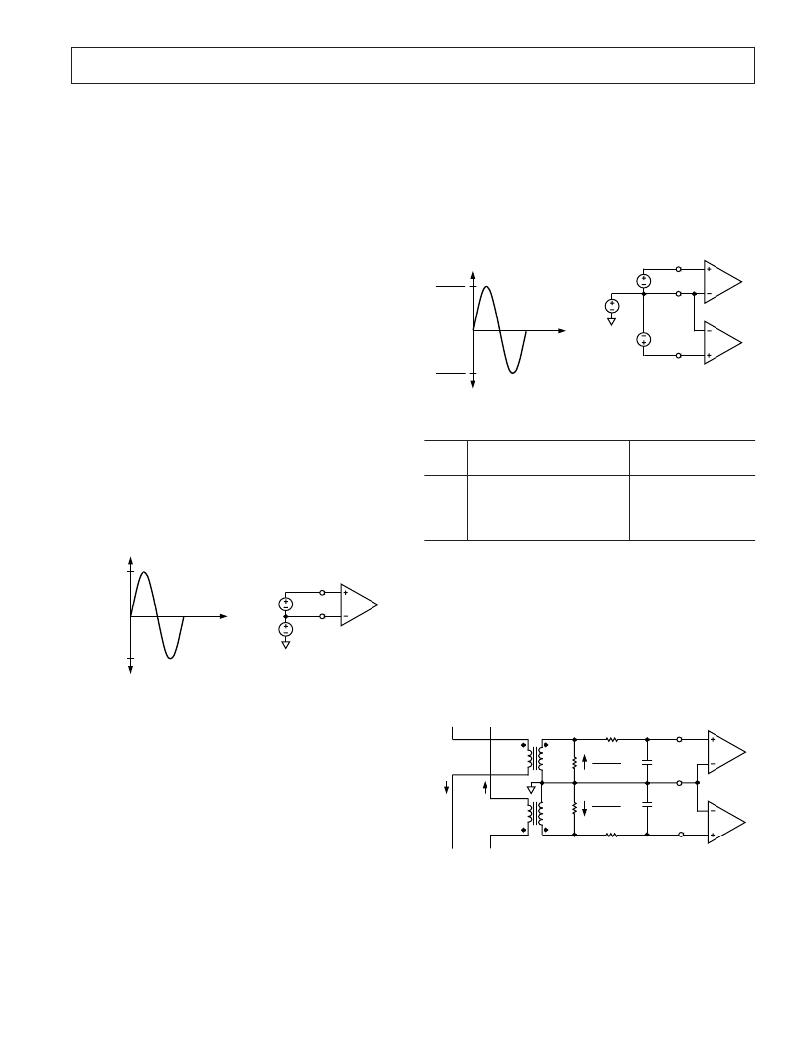
�Figure� 5� illustrates� the� maximum� signal� levels� on� V1A,� V1B,�
�and� V1N.� The� maximum� differential� voltage� is� ±� 660� mV� divided�
�by� the� gain� selection.� Again,� the� differential� voltage� signal� on� the�
�inputs� must� be� referenced� to� a� common� mode,� e.g.,� AGND.� The�
�maximum� common-mode� signal� is� ±� 100� mV� as� shown� in� Figure� 5.�
�φ� h� =� α� h� –� β� h�
�As� shown� in� Equation� 5� above,� a� harmonic� real� power� compo-�
�V1A,� V1B�
�+660mV�
�GAIN�
�DIFFERENTIAL� INPUT� A�
�660mV/GAIN� MAX� PEAK�
�V1�
�V1A�
�nent� is� generated� for� every� harmonic,� provided� that� harmonic� is�
�present� in� both� the� voltage� and� current� waveforms.� The� power�
�factor� calculation� has� been� shown� previously� to� be� accurate� in�
�V� CM�
�COMMON� MODE�
�100mV� MAX�
�V� CM�
�AGND�
�V1N�
�the� case� of� a� pure� sinusoid,� therefore� the� harmonic� real� power�
�must� also� correctly� account� for� the� power� factor� since� it� is� made�
�up� of� a� series� of� pure� sinusoids.�
�–660mV�
�GAIN�
�DIFFERENTIAL� INPUT� B�
�660mV/GAIN� MAX� PEAK�
�V1�
�V1B�
�Note� that� the� input� bandwidth� of� the� analog� inputs� is� 14� kHz�
�with� a� master� clock� frequency� of� 3.5795� MHz.�
�Figure� 5.� Maximum� Signal� Levels,� Channel� 1�
�Table� I.�
�ANALOG� INPUTS�
�Channel� V2� (Voltage� Channel)�
�Maximum�
�The� output� of� the� line� voltage� transducer� is� connected� to� the�
�ADE7751� at� this� analog� input.� Channel� V2� is� a� fully� differen-�
�tial� voltage� input.� The� maximum� peak� differential� signal� on�
�Channel� 2� is� ±� 660� mV.� Figure� 4� illustrates� the� maximum�
�signal� levels� that� can� be� connected� to� the� ADE7751� Channel� 2.�
�G1�
�0�
�0�
�1�
�1�
�G0�
�0�
�1�
�0�
�1�
�Gain�
�1�
�2�
�8�
�16�
�Differential� Signal�
�±� 660� mV�
�±� 330� mV�
�±� 82� mV�
�±� 41� mV�
�V2�
�+600mV�
�V2P�
�Typical� Connection� Diagrams�
�Figure� 6� shows� a� typical� connection� diagram� for� Channel� V1.�
�V� CM�
�DIFFERENTIAL� INPUT�
�600mV� MAX� PEAK�
�COMMON� MODE�
�100mV� MAX�
�V2�
�V� CM�
�V2N�
�Here� the� analog� inputs� are� being� used� to� monitor� both� the�
�phase� and� neutral� currents.� Because� of� the� large� potential�
�difference� between� the� phase� and� neutral,� two� CTs� (current�
�transformers)� must� be� used� to� provide� the� isolation.� Notice�
�–600mV�
�AGND�
�both� CTs� are� referenced� to� AGND� (analog� ground),� hence�
�the� common-mode� voltage� is� 0� V.� The� CT� turns� ratio� and�
�Figure� 4.� Maximum� Signal� Levels,� Channel� 2�
�Channel� 2� must� be� driven� from� a� common-mode� voltage,� i.e.,�
�burden� resistor� (Rb)� are� selected� to� give� a� peak� differential�
�voltage� of� ±� 660� mV/gain.�
�the� differential� voltage� signal� on� the� input� must� be� referenced� to�
�a� common� mode� (usually� AGND).� The� analog� inputs� of� the�
�ADE7751� can� be� driven� with� common-mode� voltages� of� up� to�
�100� mV� with� respect� to� AGND.� However,� best� results� are�
�CT�
�Rb�
�Rf�
�660mV�
�GAIN�
�Cf�
�V1A�
�achieved� using� a� common� mode� equal� to� AGND.�
�Channel� V1� (Current� Channel)�
�The� voltage� outputs� from� the� current� transducers� are� connected�
�IP�
�IN�
�AGND�
�Rb�
�660mV�
�GAIN�
�Cf�
�V1N�
�to� the� ADE7751� here.� Channel� V1� has� two� voltage� inputs,� namely�
�V1A� and� V1B.� These� inputs� are� fully� differential� with� respect� to�
�V1N.� However,� at� any� one� time,� only� one� is� selected� to� perform�
�PHASE� NEUTRAL�
�CT�
�Rf�
�V1B�
�the� power� calculation—see� Fault� Detection� section.�
�REV.� 0�
�–11� –�
�Figure� 6.� Typical� Connection� for� Channel� 1�
�发布紧急采购,3分钟左右您将得到回复。
相关PDF资料
EVAL-ADE7752AEBZ
BOARD EVALUATION FOR ADE7752A
EVAL-ADE7753ZEB
BOARD EVALUATION AD7753
EVAL-ADE7754EBZ
BOARD EVALAUTION FOR ADE7754
EVAL-ADE7755ZEB
BOARD EVALUATION FOR AD7755
EVAL-ADE7758ZEB
BOARD EVAL FOR AD7758
EVAL-ADE7759EBZ
BOARD EVALUATION FOR ADE7759
EVAL-ADE7762EBZ
BOARD EVALUATION FOR ADE7762
EVAL-ADE7763ZEB
BOARD EVALUATION FOR ADE7763
相关代理商/技术参数
EVAL-ADE7752AEB
制造商:Analog Devices 功能描述:EVAL BD THREE PHASE ACTIVE ENERGY MET IC - Bulk
EVAL-ADE7752AEBZ
功能描述:BOARD EVALUATION FOR ADE7752A RoHS:是 类别:编程器,开发系统 >> 评估演示板和套件 系列:- 标准包装:1 系列:- 主要目的:电信,线路接口单元(LIU) 嵌入式:- 已用 IC / 零件:IDT82V2081 主要属性:T1/J1/E1 LIU 次要属性:- 已供物品:板,电源,线缆,CD 其它名称:82EBV2081
EVAL-ADE7752EB
制造商:AD 制造商全称:Analog Devices 功能描述:Three Phase Energy Metering IC with Pulse Output
EVAL-ADE7753ZEB
功能描述:BOARD EVALUATION AD7753 RoHS:是 类别:编程器,开发系统 >> 评估演示板和套件 系列:- 标准包装:1 系列:- 主要目的:电信,线路接口单元(LIU) 嵌入式:- 已用 IC / 零件:IDT82V2081 主要属性:T1/J1/E1 LIU 次要属性:- 已供物品:板,电源,线缆,CD 其它名称:82EBV2081
EVAL-ADE7754EB
制造商:Analog Devices 功能描述:EVALUATION BOARD FOR POWER METERING, POLYPHASE MULTIFUNCTION ENERGY METERING IC WITH SERIAL PORT 制造商:Analog Devices 功能描述:PWR METERING, POLYPHASE MULTIFUNCTION ENERGY METERING IC W/ - Bulk
EVAL-ADE7754EBZ
功能描述:BOARD EVALAUTION FOR ADE7754 RoHS:是 类别:编程器,开发系统 >> 评估演示板和套件 系列:- 标准包装:1 系列:- 主要目的:电信,线路接口单元(LIU) 嵌入式:- 已用 IC / 零件:IDT82V2081 主要属性:T1/J1/E1 LIU 次要属性:- 已供物品:板,电源,线缆,CD 其它名称:82EBV2081
EVAL-ADE7755EB
制造商:Analog Devices 功能描述:EVAL BOARD ENERGY METERINGW/PULSE OUTPUT - Bulk
EVAL-ADE7755EBZ
制造商:AD 制造商全称:Analog Devices 功能描述:Energy Metering IC with Pulse Output